New White Paper: LED Illumination for Optical Semiconductor Inspection & Metrology
As semiconductor devices become smaller, denser and more complex, optical inspection systems are being asked to deliver higher sensitivity, greater repeatability and faster throughput. This is especially important as the industry continues to move towards heterogeneous integration, chiplets, 2.5D and 3D architectures, through-silicon vias and stacked die.
These developments are creating new inspection challenges. Tool developers now need illumination systems that can support a wider range of wavelengths, deliver stable output over long periods and integrate easily into increasingly sophisticated optical platforms.
Our new white paper, LED Illumination for Optical Semiconductor Inspection & Metrology, examines how LED technology can support these requirements.
Supporting advanced packaging inspection
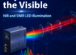
A key theme of the white paper is the growing need for NIR and SWIR illumination.
Advanced packaging applications often require inspection beyond the surface. Through-wafer inspection, bond inspection, solder bump morphology analysis, encapsulation quality verification and TSV quality control can all benefit from carefully selected wavelengths across the UV, visible, NIR and SWIR regions.
For OEMs and tool developers, this makes illumination architecture an increasingly important design decision. Flexibility across multiple wavelength regions can help inspection systems adapt to different materials, structures and process requirements.
Introducing the CoolLED Amora Series
The white paper also introduces the CoolLED Amora Series, a configurable OEM LED illumination platform designed for demanding optical instruments.
The Amora Series supports a broad wavelength range and can be tailored to specific system requirements, making it suitable for semiconductor inspection, metrology and other high-performance imaging applications where stability, control and integration are critical.

Read the full white paper
The full white paper explores the technical and commercial case for LED illumination in greater detail, including wavelength regions, inspection applications, source comparisons and cost-of-ownership considerations.
For OEMs, system builders and tool developers working in semiconductor inspection and metrology, it provides a useful overview of why LED illumination is becoming an enabling technology for the next generation of optical tools.