
Light is essential throughout semiconductor manufacturing and processing. In photolithography, EUV (Extreme Ultraviolet) and DUV (Deep Ultraviolet) light are used to create extremely fine circuit patterns on silicon wafers. Across the wider production process, UV, visible, NIR and SWIR (Short-Wave Infrared) wavelengths also play an important role in wafer inspection and metrology.
With the semiconductor industry growing rapidly, driven by AI, data centres and the EV market, manufacturers are under pressure from two directions at once:
· Higher wafer volumes
· Growing device complexity
Those demands are pushing inspection and metrology tools to work harder, with greater precision, better repeatability and faster throughput all becoming more important. Illumination is part of that picture too, especially where lamp-based technologies are still in use.
Can LEDs rise to the challenge? Yes, LED illumination can be a strong fit for semiconductor inspection and metrology.
LED illumination for semiconductor inspection and metrology
A well-designed LED illumination system can deliver precise wavelength control, stable and uniform output, support for multispectral imaging, and the flexibility needed for OEM integration.
In the right applications, LEDs now present clear benefits compared with traditional halogen, xenon and laser-induced plasma light sources. With wavelength coverage from 340 to 1900 nm, up to 10 independently controllable channels, and multiple light delivery options, LED illumination can be configured to suit the demands of modern semiconductor inspection and metrology systems.
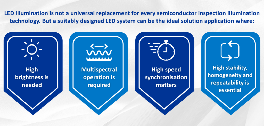
Why use LED illumination for semiconductor inspection?
Semiconductor inspection systems are built to pick up tiny features, contamination, subtle defects and critical variations in materials, surfaces and layers. The quality and consistency of the illumination plays a big part in the quality of the inspection result, which can then affect yield, throughput and overall line efficiency.
This is one of the key reasons LED illumination has become so valuable.
LEDs can deliver broadband illumination where it is needed, but there are also real advantages to working with narrower wavelength ranges. They allow engineers to select the wavelengths that are genuinely useful for a given inspection task, rather than using more light than necessary. That can improve contrast, make defects easier to see and analyse, and help create more efficient system designs.
Where precision, control and repeatability really matter, LEDs are often a better fit than older lamp technologies.
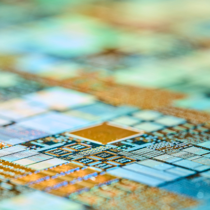
Why wavelength control matters in semiconductor metrology
In metrology, confidence comes from consistency. The more tightly optical conditions can be controlled, the more dependable the measurement result is likely to be.
One of the key strengths of LED illumination is accurate wavelength selection. Our LED systems can support a broad range of semiconductor inspection and metrology techniques across UV, visible, NIR and SWIR wavelengths.
That matters because different wavelength ranges reveal different information:
UV: fine surface detail, contamination and subtle defects
Visible: high-contrast imaging for alignment and machine vision
NIR/SWIR: deeper material interaction, layer differentiation and enhanced contrast
With LEDs, the illumination can be matched to the measurement requirement, rather than asking the measurement to adapt to the limitations of the light source.
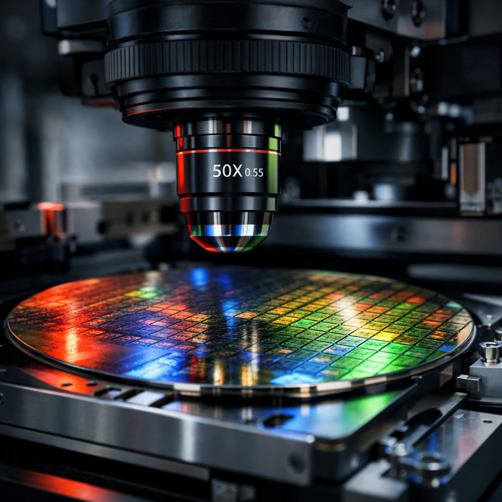
LED illumination for multispectral semiconductor inspection
As semiconductor devices become more advanced, inspection systems often need to capture information in several different ways. That usually means using more than one wavelength.
LED illumination is a strong fit for multispectral inspection because different wavelengths can be controlled independently and switched quickly. With up to 10 independently controlled channels, users can sequence wavelengths in software, fine-tune the intensity of each channel, and build repeatable illumination routines for automated inspection.
This can help systems:
- improve contrast between layers
- differentiate materials more effectively
- make subtle surface or structural defects easier to detect
- support consistent analysis from one inspection to the next
For metrology systems, independent channel control also helps maintain reliable, repeatable measurement conditions.
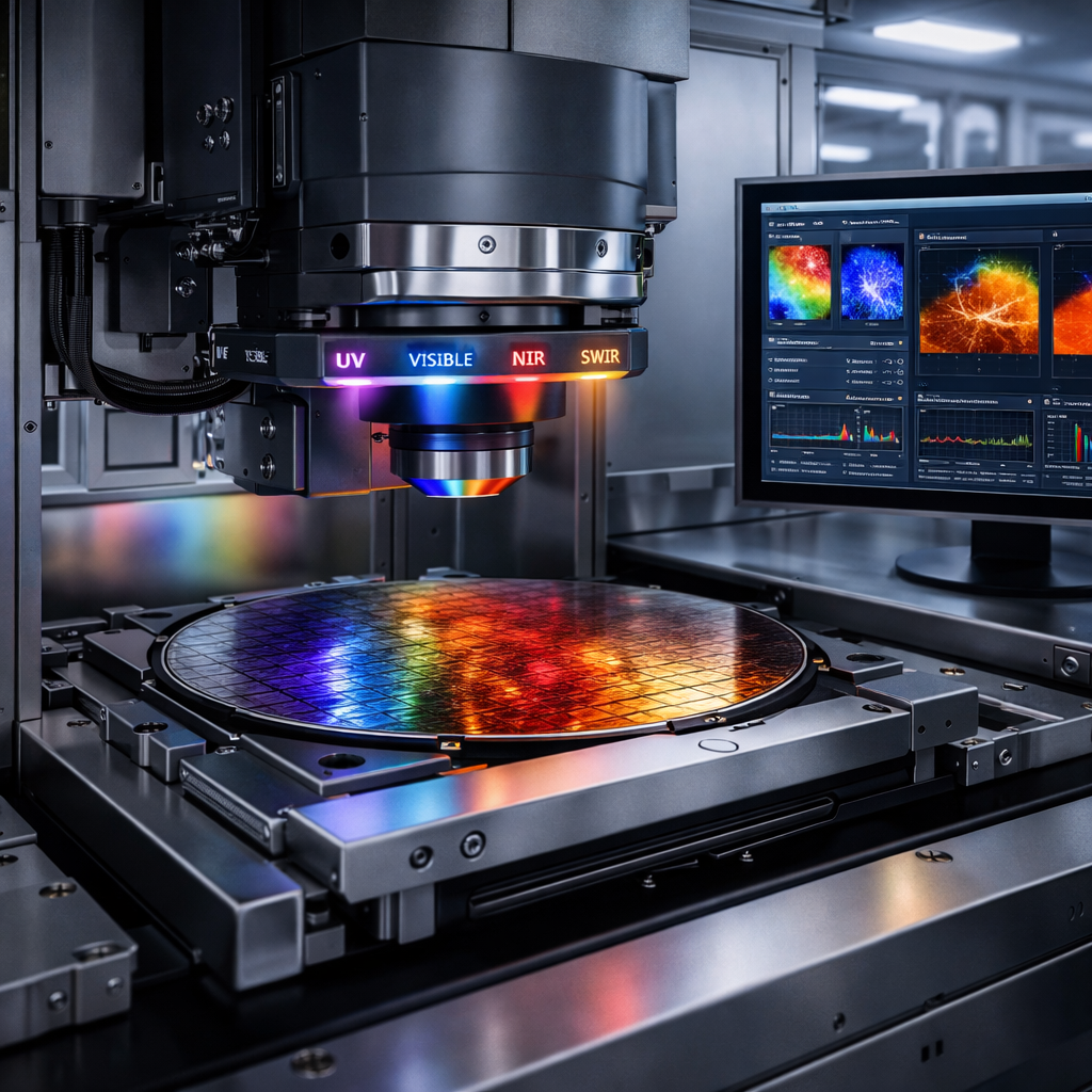
Flexible light delivery for OEM semiconductor and metrology tools
Semiconductor inspection systems are often highly customised, which means the illumination system needs to integrate easily into specialised optical designs.
That makes light delivery an important consideration. LED systems can be configured in a range of ways to provide the most practical and efficient solution, including:
- direct coupling
- fibre optic or liquid light guide delivery
- custom optical configurations
This gives OEM designers more flexibility when developing compact inspection heads, enclosed metrology systems and bespoke OEM platforms.
Rather than making the tool design conform to the light source, LED illumination can be tailored to fit the application.
For metrology and semiconductor inspection applications centred on precision, repeatability and performance tailored to the task, LEDs are often not merely suitable, but the most appropriate choice.
Can LEDs replace halogen and Xenon bulbs in semiconductor inspection?
In many cases, yes. For semiconductor inspection and metrology systems, LED illumination can offer longer lifetime, no warm-up delay, lower maintenance, and more precise control over wavelength and intensity, making it a very strong alternative.
Are LEDs good for semiconductor metrology?
Yes. LED illumination can deliver the stability, repeatability and wavelength-specific control required for consistent optical measurement.
What is the best light source for semiconductor inspection?
The best light source depends on the application. That said, LED illumination is often a strong choice for workflows that require precise wavelength control, multispectral capability, stable output and flexible OEM integration.
What wavelengths are used in semiconductor inspection and metrology?
The wavelengths used depend on the application. Semiconductor inspection and metrology may involve UV, visible, NIR and SWIR wavelengths depending on the material being examined, the structure involved, the type of defect, or the measurement goal. LED illumination from 340 to 1900 nm can support many of these approaches, with broadband output available where required.
Can LEDs be used for multispectral semiconductor inspection?
Yes. LED systems can be configured with multiple channels that can either be combined for broadband illumination or controlled independently for multispectral semiconductor inspection, supporting fast wavelength switching and repeatable illumination sequences.