

CoolLED at Semicon Europa 2026 – LED Illumination for Inspection and Metrology
CoolLED returns to SEMICON Europa 2026 to discuss advances in LED illumination for semiconductor inspection, wafer imaging and optical metrology

CoolLED returns to SEMICON Europa 2026 to discuss advances in LED illumination for semiconductor inspection, wafer imaging and optical metrology
Why pulsed xenon has powered semiconductor inspection for decades, and why OEMs are increasingly turning to LED illumination instead
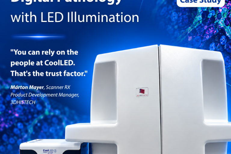
Find out how CoolLED and 3DHISTECH have partnered to advance fluorescence imaging performance, speed and consistency in digital pathology
CoolLED and 3DHISTECH combine specialist LED illumination and digital pathology expertise to support faster, consistent fluorescence slide scanning

CoolLED heads to ISIG Korea and SEMICON Taiwan to share custom LED illumination from 250 to 2000 nm for semiconductor inspection and metrology
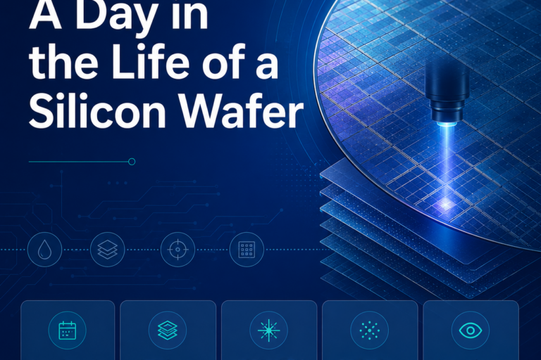
Follow a silicon wafer through months of lasers, plasma, microscopic layering and LED inspection to see how one of humanity’s most ridiculous manufacturing feats becomes a working semiconductor.

As we look into 2026, our goals are simple, even if the work itself is complex…

Meet CoolLED at SPIE BiOS and Photonics West 2026 to explore custom OEM LED Illumination built for a huge range of applications
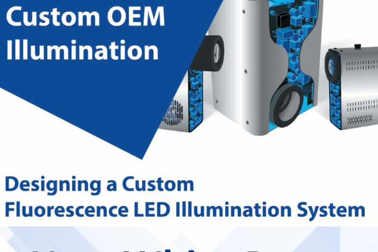
In the world of microscopy, it’s tempting to think that “lighting up a sample” is trivial. After all, anyone can point a light at a slide… right?
Need something a little different?
For manufacturers who wish to gain a competitive advantage through bright, stable and controllable illumination, CoolLED’s world-renowned LED technology is available in customised configurations.

Did you know that LED illumination systems help laboratories reduce their carbon footprint, protecting laboratory staff along the way?
Toxic mercury-based microscope illuminators are bad news for the environment, draw a lot of power and have a short lifetime.
LED illumination systems are cleaner, have a long lifetime and use less power. Our pE-300 Series is also ACT label certified and is a natural choice for labs who want to play their part in helping the environment.
At CoolLED we are committed to giving our customers outstanding service right from the start and throughout the lifetime of the product. Please get in touch if you have any questions or would like a quote. You can also browse our site for technical resources and general support.