Where LEDs Power Semiconductor Inspection
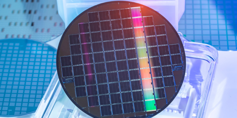
Semiconductors are in everything – phones, cars, even your fridge. Making them, though, is another story. Tiny defects can cause massive failures, so inspection and metrology (fancy word for precise measurement) are essential at almost every stage of production.
LEDs don’t replace every light source in semiconductor fabs but, in the right places, they’re becoming the unsung heroes. Let’s look at five key stages where LEDs are used, and why.
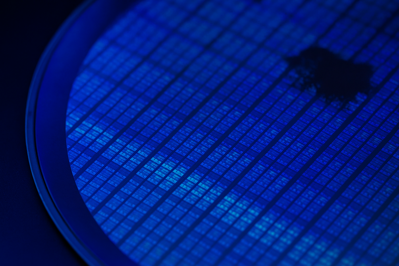
1. Wafer Surface Inspection
Technical speak: Detecting particles, scratches, or residues on the wafer surface using brightfield and darkfield illumination. Stable, homogenous lighting ensures surface defects are visible for both visual and automated detection.
Layman’s terms: Imagine cleaning your glasses and holding them up to a bright window. Any smudges or scratches instantly show up. That’s what LEDs do for wafers, making sure the surface is spotless before the next process.

2. Photomask & Lithography Alignment
Technical speak: During photolithography, precise alignment of wafer layers is critical. While exposure still uses lasers or arc lamps, LEDs are sometimes used as the illumination source for detecting alignment marks because of their spectral stability and wavelength flexibility.
Layman’s terms: Think of it like trying to line up two transparencies perfectly. The actual “printing” still needs a specialist lamp, but LEDs provide the lighting to check everything is lined up properly before you press “go.”

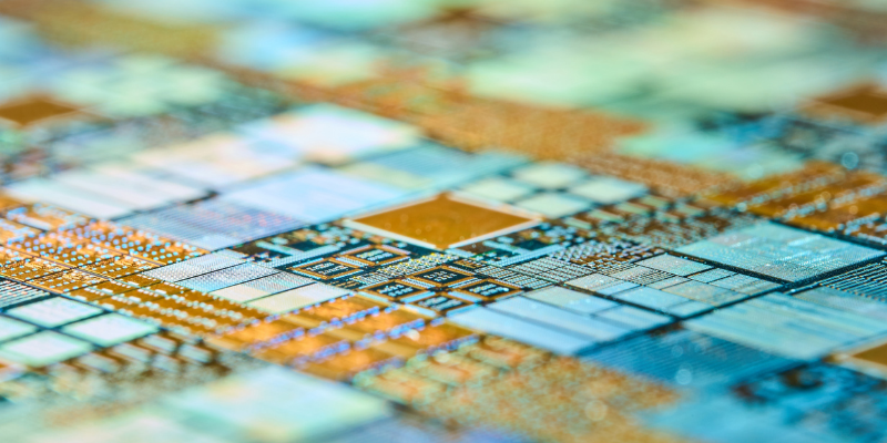
3. Defect Inspection & Pattern Recognition
Technical speak: Using LED illumination at multiple wavelengths to reveal pattern defects, missing features, or bridging in fine circuits. LEDs enable repeatable conditions for automated optical inspection (AOI).
Layman’s terms: Picture checking a knitted jumper for dropped stitches but on a microscopic scale. LEDs highlight missing or misaligned “stitches” in circuits, ensuring every pattern is intact.

4. Critical Dimension Metrology
Technical speak: Measuring linewidths, spaces, and feature sizes on wafers using imaging and scatterometry. LEDs provide narrowband, stable illumination that helps detect nanometre-scale variations.
Layman’s terms: It’s like measuring the thickness of a human hair with a ruler, but instead if inches and centimetres, or even millimetres, we’re talking nanometres. LEDs give precise, stable light so measurement tools can tell if a circuit line is too wide or too narrow.

5. Packaging & Final Inspection
Technical speak: LED illumination is widely used in back-end processes such as die bonding and packaging inspection, where solder bumps, wire bonds, and encapsulations are checked for uniformity and defects.
Layman’s terms: Imagine quality-checking chocolates in a box: are they all the right shape, coated properly, and free from cracks? LEDs do the same for chips, making sure every “finished product” is perfect before it ships out.

👉 The takeaway: LEDs aren’t everywhere in semiconductor production, but where stability, repeatability and uptime matter – surface inspection, AOI, packaging, and as support in alignment/metrology – they’re becoming the trusted choice
Written by Ben Furness / [email protected] / LinkedIn Profile


