CoolLED for Semiconductor Inspection
2025 has been a landmark year for CoolLED’s growing presence in the semiconductor inspection space. As demand increases for stable, uniform and energy-efficient illumination in wafer inspection, mask alignment, defect analysis and automated optical inspection (AOI), our solid-state LED technology continues to offer a compelling alternative to conventional light sources.
This year we showcased that capability across major SEMICON events around the world, building new relationships, strengthening existing ones and demonstrating how LED illumination is evolving to meet the needs of high-precision semiconductor inspection.
SEMICON Taiwan
Our first major semiconductor event of the year was SEMICON Taiwan, where we exhibited as part of a wider initiative to highlight the value LEDs bring to inspection and metrology. The booth saw steady traffic from equipment manufacturers, integrators and component suppliers keen to explore alternatives to traditional illumination.
With increasing pressure on fabs to reduce running costs and move towards more sustainable, mercury-free technologies, our LED light sources attracted interest for their reliability, long lifetime and low maintenance demands which are all crucial factors in high-volume manufacturing settings.
SEMICON West
Following Taiwan, the team headed to SEMICON West in San Francisco, where discussions centred around integration. Many OEMs and system builders are now looking for illumination solutions that are:
-
Compact and easy to integrate,
-
Stable over long operating cycles,
-
Customisable with narrow spectral outputs, and
-
Compatible with fibre delivery or collimated light paths.
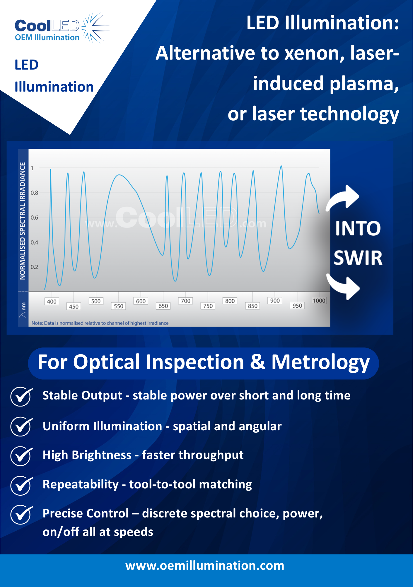
These requirements match perfectly with our Amora custom OEM illumination which offer precise wavelength control, rapid switching, and class-leading stability for inspection tasks.

SEMICON Japan: Next stop
To round off the year, CoolLED will be attending SEMICON Japan – this time with our top OEM team on the ground.
Technical Director Gerry Whoriskey will be joined by Head of Marketing and Business Development Liz Stark, continuing our commitment to supporting semiconductor manufacturers and equipment companies as they transition away from traditional light sources.
SEMICON Japan will be an opportunity to deepen conversations that began earlier in the year, particularly around higher-performance OEM builds, wavelength-specific illumination and custom solutions for AOI and defect analysis.
Where CoolLED LEDs fit into semiconductor inspection
Semiconductor inspection often demands a mix of speed, precision and spectral consistency. CoolLED illumination systems excel across core areas such as:
Wafer and Die Inspection
Our LEDs provide uniform, stable illumination that is essential for surface analysis, crack detection and particulate assessment.
Mask and Photomask Alignment
Fast switching and consistent wavelength output support alignment processes where precision and low drift are essential.
Automated Optical Inspection (AOI)
LEDs deliver repeatable and reliable illumination for automated defect detection, supporting high-speed cameras and advanced optical setups.
Metrology & Optical Characterisation
Where consistent spectral output is required for repeatable measurements, our LED systems offer low noise, long lifetime and minimal heat output.
Machine Vision in Packaging and Bonding
Compact form factors and excellent integration options make our light sources ideal for packaging lines where space is at a premium.
Across all these areas, our solutions help customers reduce downtime, avoid consumable costs associated with mercury and metal-halide lamps, and deliver the level of repeatability that semiconductor manufacturing demands.


